In 2004 I was working for Microsoft in the Xbox group, and a new console was being created. I got a copy of the detailed descriptions of the Xbox 360 CPU and I read it through multiple times and suddenly I’d learned enough to become the official CPU expert. That meant I started having regular meetings with the hardware engineers who were working with IBM on the CPU which gave me even more expertise on this CPU, which was critical in helping me discover a design flaw in one of its instructions, and in helping game developers master this finicky beast.
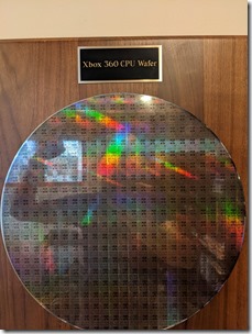
It was a lot of fun, and the work was appreciated, so a few months before  the console shipped I got a present from the leadership of the project – an entire silicon wafer of Xbox 360 CPUs! That 30 cm disk of dice (I’ve always preferred “dice” as the plural form of CPU “die”) has been hanging on my home-office wall ever since. At its largest extent it has 23 complete CPUs horizontally and 20 vertically, but much fewer than 460 CPUs total due to the circular shape of the wafer. A lot of CPUs are partially or totally omitted because of that – I counted 356 complete CPUs on the wafer.
It looks cool, it creates beautiful rainbow diffraction effects, and the individual chips are big enough that you can see the key features of the CPU that occupied my career for five years.
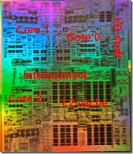
 The Xbox 360 CPU had three PowerPC cores and a 1 MB L2 cache and these features are clearly visible on the wafer.
In the die picture to the right (which looks to be about 14 mm by 12 mm) you can see the regular pattern of small black rectangles in the bottom right corner – that’s the L2 cache. To the left of that is one of the CPU cores. Above that but flipped vertically is another CPU core, and to the right of that one and flipped horizontally is the third CPU core. I used to know what the visible elements of the CPU cores were (L1 caches? register files? arithmetic units?) but I’ve long since forgotten. However they are still distinctive enough to make the reflective copying obvious.
 In addition to the three CPU cores and the L2 cache there is a horizontal bar going across the middle of the chip, and some more space to the right of the top-right CPU. I think that the horizontal bar is the bus that connects the CPUs to each other and to the L2 cache, and the top-right stuff is presumably for off-chip I/O.
The picture to the right – beautifully annotated by yours truly – is literally just a cell-phone picture of the wafer hanging on my wall. I may be biased – or traumatized by my time dealing with this ornery CPU – but I think that being able to see the features of this chip so clearly is wonderful.
So, this is all very pretty, and I know that you all wish you had one of these on your wall, but there is more to tell. Back in the day I wrote a lot of benchmarks in order to look for places where the actual performance of the CPU didn’t match what we expected. I remember doing that for our customized memcpy routine and discovering that prefetch instructions that missed in the TLB (Translation Lookaside Buffer, also known as the  page-table cache) were discarded. Since we typically prefetched about 1 KiB (eight 128-byte cache lines) ahead this meant that when copying large amounts of memory (where every 4 KiB page would give a TLB miss) roughly 25% of prefetches would be discarded. Those cache-line reads would then be handled serially, instead of having eight happening in parallel, causing large memory copies to take almost three times as long. These discarded prefetches were particularly bad because the Xbox 360 CPU was an in-order processor so no work would be done while waiting on the non-prefetched reads. This lead to me rewriting the heap so that it would use 64-KiB pages, thus avoiding most of the TLB misses and restoring the expected performance.
So, anyway. I wrote a lot of benchmarks.
One benchmark I wrote measured the L2 cache latency. This is done by setting up a linked list, following the links, and seeing how many cycles it takes to walk a long list. With fixed hardware it’s easy to construct a linked list that will stay in L1, or will always require a trip to L2, or will always require a trip to main memory. Standard stuff.
I don’t remember what the L2 cache latency was but do remember that the latency varied depending on which CPU core I ran it on. The L2 latency from CPU core 0 was pretty reliably four cycles lower than the L2 latency from CPU core 1 or 2. So that’s interesting.
 As I mentioned earlier, all communication between the CPU cores and the L2 cache was done through that horizontal strip across the middle of the chip. That means, necessarily, that all of the L2 traffic came out through the top of the L2 cache and then made its way to the three different CPUs. I’ve zoomed in on the earlier CPU die picture and added some arrows showing the flow of information from the L2 cache to the three different CPU cores. The crucial thing is that the path to the top-right CPU is quite short, whereas the path to the two CPUs on the left is noticeably longer – the signals have to travel horizontally across the interconnect.
The horizontal black lines on the very left are the millimeter markers (ask a Canadian friend if you’re not familiar with these units) on a ruler that I held against the wafer when I took the picture. I rotated that ruler image and used it to measure the length of my horizontal red line and it came in at 5.5 mm. Since the Xbox 360 CPU ran at 3.2 GHz and since CPU cores 1 and 2 had an extra four cycles of L2 latency we can conclude that it took 1.25 nanoseconds for the signals to propagate that 5.5 mm distance!
Update: the day after publishing I realized that the extra four cycles of L2 is probably two extra cycles for the request to go from the CPU to L2, and then two extra cycles for the reply. So the 5.5 mm actually only takes 0.625 nanoseconds each way, the signal actually goes 11 mm in 1.25 nanoseconds, so the original title of this blog post is a lie. Sorry!
Light can travel roughly 30 cm in one nanosecond so you may be wondering why this signal is traveling so slow. I will try to answer this but I must warn that I am a software developer with no formal training in hardware, so I might be misleading or wrong.
One reason is simply that electrical signals in wires, especially very thin wires, do not travel at the speed of light. Another reason is that the signal is not traveling continuously. Instead the signal travels a short distance and then is latched by some gates and then on the next clock cycle it travels a bit farther, so the poor signal never even has a chance to get up to full speed. Finally, the Xbox 360 was designed to run at a higher clock speed, but then shipped at 3.2 GHz because otherwise it would have melted. The 5.5 mm in four clock cycles was probably an artifact of the design goal of having the clock cycles be much shorter.
That said, 5.5 mm in 1.25 nanoseconds is still about 4,400 kilometers per second (actually 8,800 km/s, see the update above), so it’s not exactly slow. I mean, it’s 53 billion furlongs per fortnight, which seems pretty fast. But mostly I just inordinately geekily love that I can see that 1.25 nanosecond delay, with my naked eye, hanging on my wall. Thanks Xbox leadership!
Aside
 The origin story above for how I became the Xbox 360 CPU expert is reasonably accurate. I was never assigned the task of becoming CPU expert, I was just given access to the reading material and I studied it to a slightly fanatical degree. I remembering lying on our living room floor during a snowpocalypse-triggered power outage reading it by flashlight until all the pipeline quirks made sense. This same learning pattern has been true for many areas of expertise that I have grabbed, from crash analysis to floating point to compiler bugs to CPU bugs. It’s worked for me.
如有侵权请联系:admin#unsafe.sh