Xiaomi's MJA1 is a proprietary secure chip used i 2026-6-17 22:0:0 Author: blog.quarkslab.com(查看原文) 阅读量:0 收藏
Xiaomi's MJA1 is a proprietary secure chip used in their recent cameras to protect sensitive data and device communications. With no public documentation available, we conducted a black-box security analysis covering hardware identification, I2C sniffing, flash dumping, and firmware reverse engineering. This post walks through how we mapped the chip's command protocol, brute-forced undocumented commands, and assessed its security properties.
Discovery of MJA1 secure chip
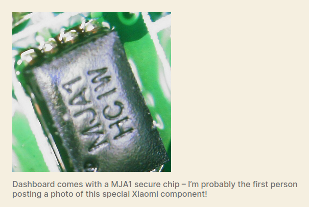
When navigating on Xiaomi's online store to find a new R&D target, we ended up on a description of the MJA1 secure chip, available on their recent cameras.

This chip claims to provide hardware-level protection for sensitive data and device communications. It is designed to be resistant to a variety of common attacks, including replay attacks, MITM attacks, brute force, ... And each chip has its own private key and certificate.
However, it is a proprietary chip: no documentation or datasheet is present on the Internet. At the time of writing, no public research work has been done on it, only a picture from RoboCoffee1.
With no public information available, our goal for this project was to understand how the MJA1 secure chip works and evaluate its security properties through black-box analysis.
Target identification
The first step was to find a target satisfying the following criteria:
- Integrating the MJA1 secure chip;
- Reasonable price (< 50-100€);
- Allowing firmware upgrades interception, via mobile app for example, in case we fail to dump the firmware.
We ended up purchasing two devices for the price of one:
They both have a MJA1 secure chip integrated and can interact together. This way, we can compare two different devices, check for the easiest target, and cross-validate our findings.
Hardware analysis
MJA1 secure chip identification
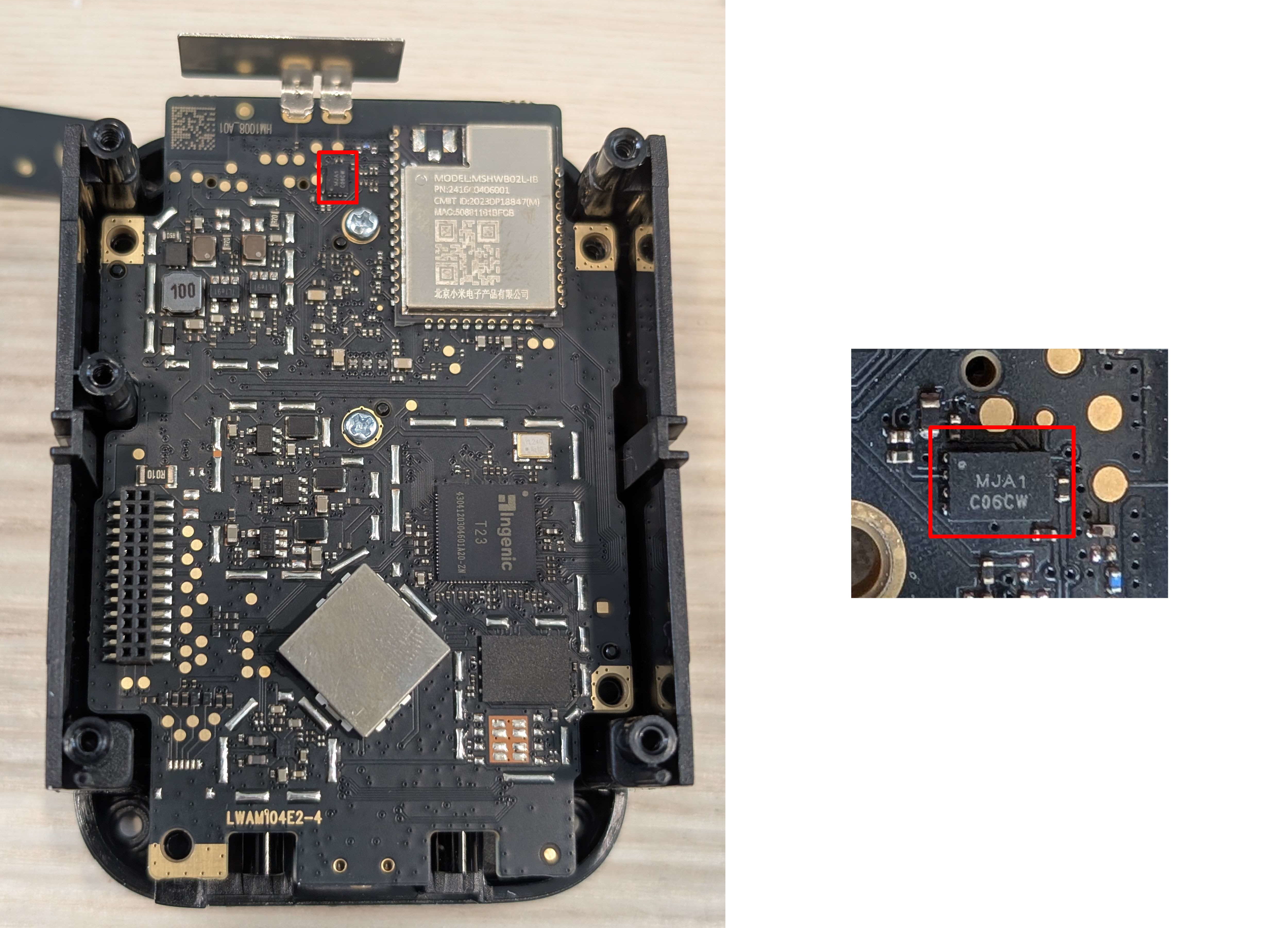
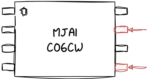
After opening both devices and inspecting their PCBs, we located the MJA1 chip on each board.
Both devices use the same MJA1 C06CW model.
The following picture shows the MJA1 chip on the BW300 camera.
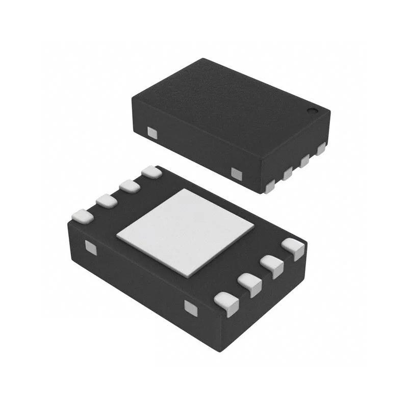
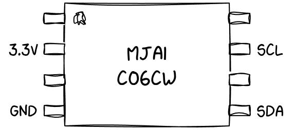
The chip comes in a DFN 2×3-8 package, which means:
- Dual Flat No-lead (DFN);
- Size: 2 × 3 mm 🤏;
- 8 pins.
To identify the communication interface, we had to actively probe the chip while the device was running.
Sniffing communications
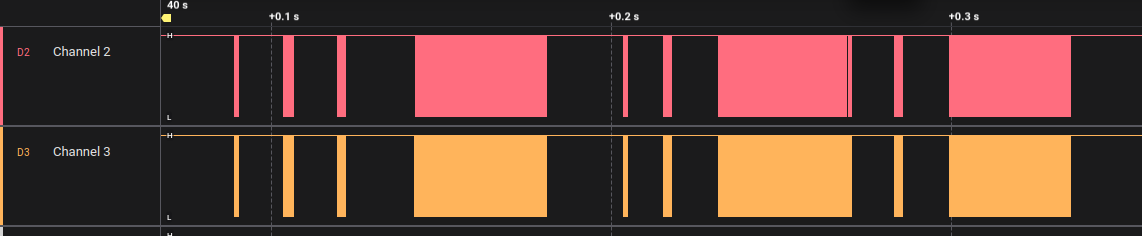
To observe the communication between the main SoC and the MJA1 chip, we used a PCBite setup combined with a logic analyzer. The PCBite probes can easily fit onto the 0.5 mm pin pitch of the chip.
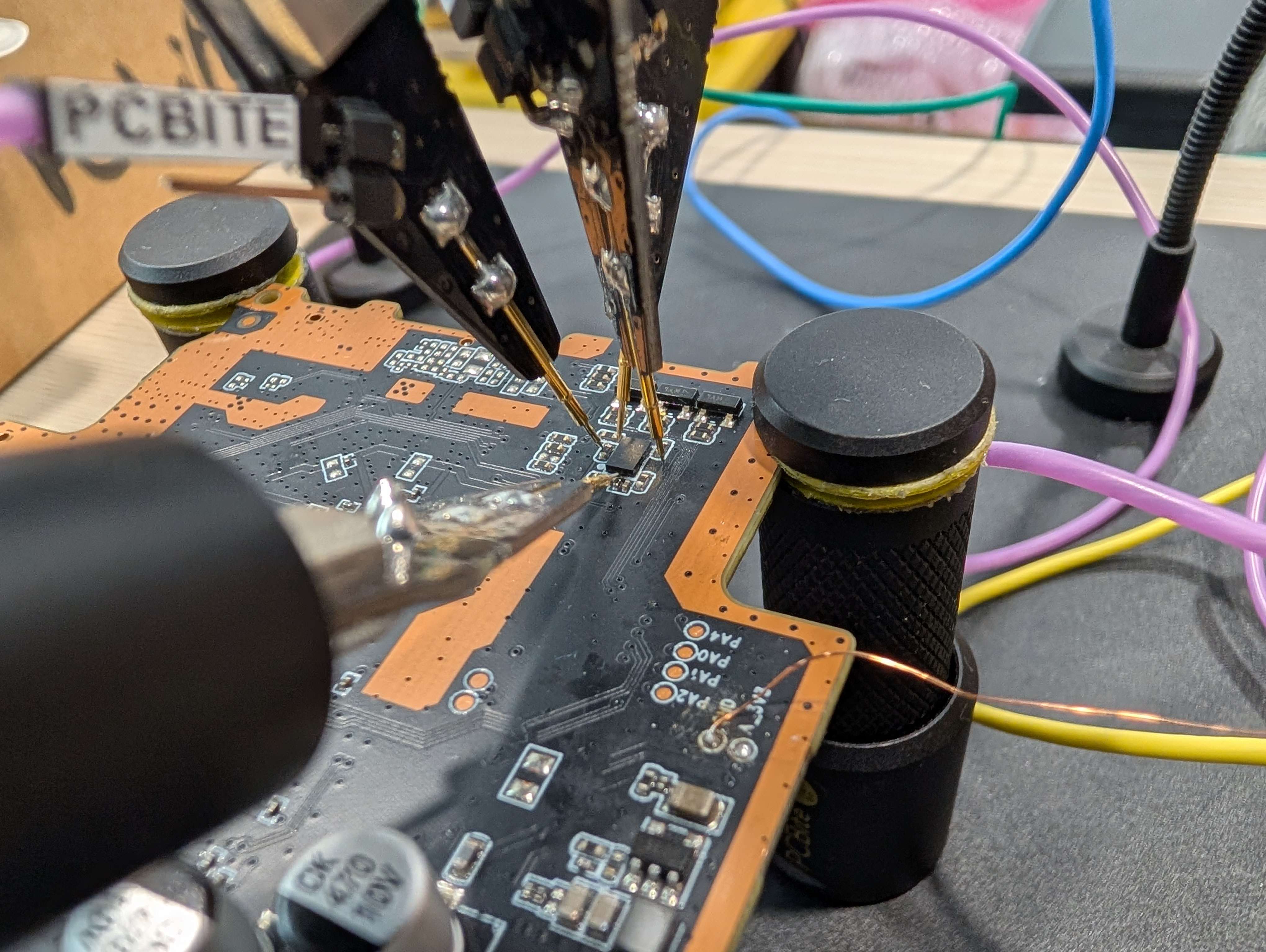
We then powered the camera base station and started capturing signals on the pins of the chip. The goal at this stage was simple: identify which pins carried data, and from there, figure out what protocol was used.
Looking at the eight pins, most of them stayed flat, which may indicate VCC/pull-ups (constant high) or GND (constant low). Only two showed active data exchange:
In the embedded world, most common interfaces have characteristic pin counts:
- UART uses two pins (TX, RX), but both are active in different directions and in an asynchronous way;
- SPI needs at least four pins (CLK, MOSI, MISO, CS), which does not correspond to our case;
- I2C uses exactly two pins (SCL, SDA), shared bidirectionally between master and slave, synchronously.
Zooming in on the captures revealed the typical signature of an I2C bus, with a regular clock line and a data line:
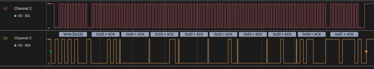
By applying the built-in I2C decoder of the logic analyzer, we could read the transaction: Write [0x2A] to address the chip, then a sequence of data bytes: 0x05, 0x00, 0x03, 0x00, 0x02, 0x00, 0x08, 0x58, 0xEF, each acknowledged by the slave.
From there, we could conclude:
- Communication with the secure chip uses the I2C protocol;
- The clock (SCL) defines when data is read; the data line (SDA) carries the bits;
- The address of the secure chip is 0x2A — I2C being a shared bus, each device on it is identified by such an ID.
As a side note, the exact byte sequence captured above (0x05 0x00 0x03 0x00 0x02 0x00 0x08 0x58 0xEF) is in fact a READ command, the very same one we will decode in detail later in this post.
Sniffing gave us the transport layer, but the actual command structure on top of I2C was still unknown. To understand it, we needed to extract and analyze the firmware of the host device that talks to the chip.
Flash dumping
We had two devices to work with, each with a different flash chip.
The Xiaomi Base Station has an MD25Q128 flash memory, supported by the TNM5000 universal programmer we had. The dump was therefore straightforward.
The Xiaomi Outdoor Camera BW300 was equipped with a Winbond 25N01KVZEIR flash memory. This chip was not supported by the TNM5000, so we had to find another way.
25N01KVZEIR is a 1 Gbit SPI NAND flash memory, with a WSON 8x6 mm package. Its pinout can be found from the official datasheet.
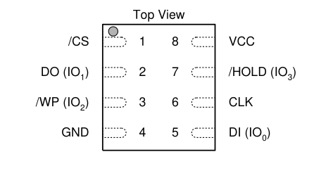
To dump unsupported SPI NAND flash, a Raspberry Pi can often be a good option. It can speak SPI directly to the chip to identify it, read raw pages, and dump the entire NAND.
The following pins of the Raspberry Pi can be used:
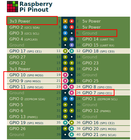
The pins can be connected like this:
| Winbond flash pin | Raspberry Pi pin |
|---|---|
| /CS | GPIO 7 (SPI0 CE1) |
| DO | GPIO 9 (SPI0 MISO) |
| /WP | 3.3V |
| GND | GND |
| DI | GPIO10 (SPI0 MOSI) |
| CLK | GPIO11 (SPI0 SCLK) |
| /HOLD | 3.3V |
| VCC | 3.3V |
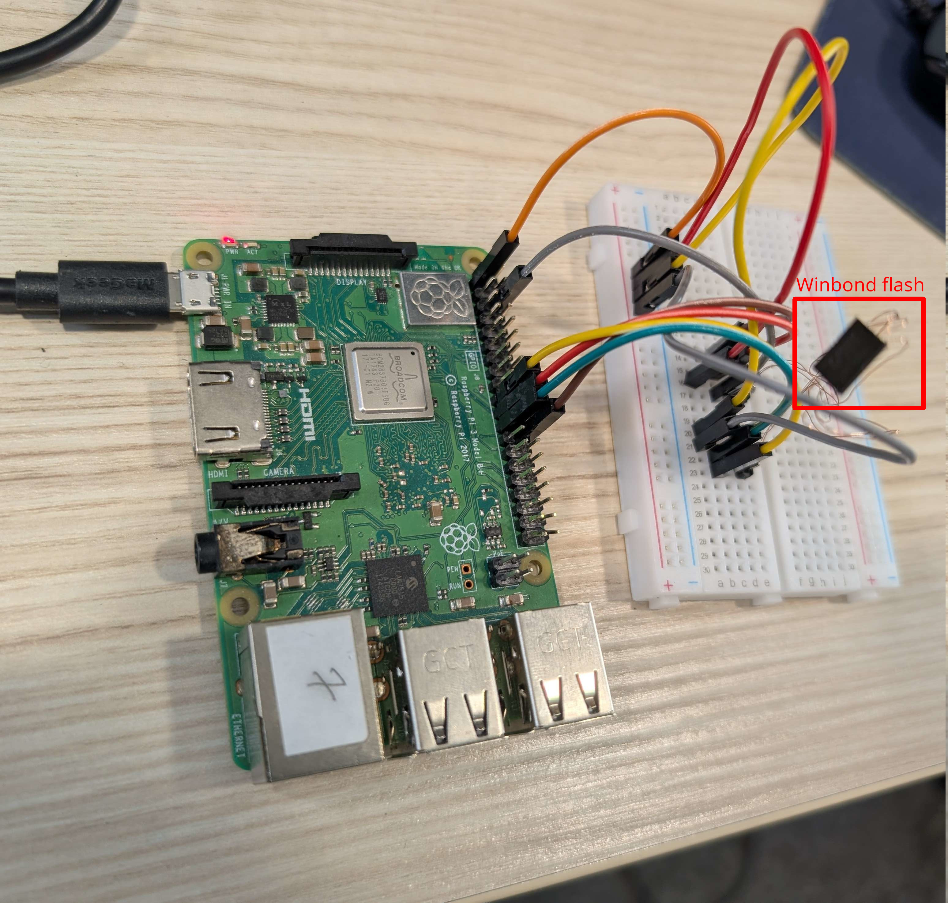
We built a custom setup based on a Raspberry Pi 3 B+, wiring the flash chip directly to the Pi's GPIO pins with a breadboard and Dupont cables.
We first read the JEDEC ID of the chip with the spidev Python module:
import spidev
import time

spi = spidev.SpiDev()
spi.open(0, 1)  # bus 0, device 1 (/dev/spidev0.1)
spi.max_speed_hz = 1000000
spi.mode = 0

# Send JEDEC ID read command (0x9F)
response = spi.xfer2([0x9F, 0, 0, 0, 0, 0, 0, 0])
print("JEDEC ID:", [hex(x) for x in response])
The ID obtained is good, according to the specification:
JEDEC ID: ['0x0', '0x0', '0xef', '0xae', '0x21', '0x0', '0x0', '0x0']
We can now proceed with dumping the entire flash binary:
import spidev
import time

# === Configuration ===
MAX_PAGE_NUMBER = 0x10000
PAGE_SIZE = 2048 # Size of data area (without spare/OOB)
SPI_BUS = 0
SPI_DEVICE = 1

# === Setup SPI ===
spi = spidev.SpiDev()
spi.open(SPI_BUS, SPI_DEVICE)
spi.max_speed_hz = 10_000_000
spi.mode = 0b00

# === Helper: Wait until NAND is ready ===
def wait_ready():
    while True:
        spi.xfer2([0x0F, 0xC0])        # 0x0F: Read status, 0xC0: Status register
        status = spi.readbytes(1)[0]
        if (status & 0x01) == 0:       # Bit 0 == 0 means "Ready"
            break
        time.sleep(0.001)

# === 1. Load page into cache using command 0x13 ===
def load_page_to_cache(page_number):
    addr = page_number.to_bytes(3, 'big')  # 24-bit address
    spi.xfer2([0x13] + list(addr))
    wait_ready()

# === 2. Read data from cache using 0x03 command ===
def read_cache_data():
    data = []
    for i in range(0, PAGE_SIZE, 4):
        addr = i.to_bytes(2, 'big')
        data += spi.xfer2([0x03] + list(addr) + [0x00, 0x00, 0x00, 0x00, 0x00])[4:]
    return data


with open("dump.bin", "wb") as f:
    for page in range(MAX_PAGE_NUMBER):
        print(f"Reading page {page}...")
        load_page_to_cache(page)
        page_data = read_cache_data()
        f.write(bytes(page_data))

spi.close()
With both firmwares extracted, we could move on to the reverse engineering phase.
Firmware analysis
Reverse engineering miio_client
Using binwalk, unblob, and SquashFS tools, we extracted the file systems from both firmwares. As expected, no code specific to the secure chip itself was found, the chip runs its own firmware, which is not exposed to the host.
Our next goal was to find, somewhere in the extracted file system, the host-side code that talks to the chip over I2C.
By looking at the strings, we found many references to the prefix mjac (MJA Chip?) inside miio_client:
$ strings mi_ot/miio_client
...
mjac_reset
mjac_get_did
mjac_get_certificate_pem
mjac_crc16_ccitt
mjac_i2c
...
MIIO refers to a proprietary set of communication protocols and SDK developed by Xiaomi for its IoT ecosystem. This binary is the one in charge of communicating with the MJA1 chip over I2C.
miio_client is a MIPS 32-bit binary, dynamically linked against uClibc, typical for an embedded Linux device:
$ file mi_ot/miio_client
mi_ot/miio_client: ELF 32-bit LSB executable, MIPS, MIPS32 rel2 version 1 (SYSV), dynamically linked, interpreter /lib/ld-uClibc.so.0, no section header
The no section header part means the binary has been stripped of its section headers, which usually makes reverse engineering harder. Luckily for us, the function names themselves had been preserved in the symbol table.
By reverse engineering this binary, we identified several relevant functions:
mjac_init: initializes the I2C interface;mjac_cmd_build_<cmd>: builds different supported commands;mjac_resp_parse_data: parses responses from the chip;mjac_crc16_ccitt: computes the CRC16 used for frame integrity.
Identified commands
By analyzing the mjac_cmd_build_* family of functions, we mapped each command ID to its purpose:
| ID | Command |
|---|---|
| 0x00 | Echo |
| 0x02 | Generate random |
| 0x05 | Read |
| 0x0D | Hibernate |
| 0x11 | Generate key |
| 0x14 | Query |
| 0x16 | Generate signature |
| 0x17 | Verify signature |
| 0x18 | Establish key |
These commands fall into three categories:
- Utility commands:
Echofor communication testing,Generate randomfor cryptographically secure random numbers,Hibernateto enter low-power mode; - Data access commands:
Readto read from specific data zones,Queryto retrieve chip information such as serial number or product version; - Cryptographic operations:
Generate key(ephemeral ECC keypair for ECDH),Establish key(shared secret derivation),Generate signature,Verify signature.
Understanding a command
Building the table above was less straightforward than it might look. Even with the function names preserved, reconstructing the exact format of each command was not trivial: each mjac_cmd_build_<cmd> function packs its arguments into a structure of magic offsets, computes a CRC over a specific range, and returns a length that is not always the same.
Take mjac_cmd_build_establish_key as an example:
int mjac_cmd_build_establish_key
              (__mjac_cmd_establish_key *_cmd, uint _cmd_len, void *_src, int _src_len)

{
  ushort crc;
  int ret;

  if (_src == (void *)0x0) {
    return 0;
  }
  if (_src_len == 0x45) {
    if (_cmd == (__mjac_cmd_establish_key *)0x0) {
      ret = 0;
    }
    else {
      ret = 0;
      if (0x48 < _cmd_len) {
        _cmd->field0_0x0 = 0x18;
        _cmd->field1_0x1 = 0xff;
        memcpy(_cmd->___key,_src,0x45);
        crc = mjac_crc16_ccitt(&_cmd->field0_0x0,0x47);
        _cmd->_crc16_lo = (char)crc;
        _cmd->_crc16_hi = (char)(crc >> 8);
        ret = 0x49;
      }
    }
    return ret;
  }
  return 0;
}
Reading this carefully reveals quite a bit about the command format:
- The first byte (
0x18) is the command ID, confirming that Establish key is command 0x18; - The second byte (
0xff) is a constant with unclear meaning; - The next
0x45bytes are the actual command payload, copied from the caller's buffer; - The CRC16 is computed over the first
0x47bytes, and appended as two little-endian bytes; - The total frame length is
0x49bytes: 1 (ID) + 1 (constant) + 0x45 (payload) + 2 (CRC).
Doing this carefully for each command was the only reliable way to recover the protocol.
Rebuilding the CRC
The integrity of every command is protected by mjac_crc16_ccitt. We needed a working implementation of it before we could send a single valid frame to the secure chip. The function name suggested a standard CRC-16/CCITT variant, but there are many of those in the wild, differing in four parameters: polynomial, initial value, whether input and output bits are reflected, and the final XOR.
By reading the decompiled function, we identified all these parameters:
- The shift-and-XOR pattern, combined with a 256-entry lookup table, pointed to a reflected CRC implementation (low byte first, right shift on the register);
- The lookup table itself encoded a polynomial of
0x8408, which is the bit-reversed form of0x1021, the canonical CCITT polynomial; - The register was initialized to
0xFFFF; - The final result was bitwise inverted before being returned.
This corresponds to the CRC-16/X-25 (also known as CRC-16/IBM-SDLC) variant. It is a standard preset but specifically not the one most people reach for when they hear "CRC-16/CCITT", which is why we had to derive it from the code rather than guess it.
We reimplemented it in C and used it later on a rooted camera to generate valid frames:
static const uint16_t crc16_table[256] = {
    0x0000, 0x1189, 0x2312, 0x329B, 0x4624, 0x57AD, 0x6536, 0x74BF,
    0x8C48, 0x9DC1, 0xAF5A, 0xBED3, 0xCA6C, 0xDBE5, 0xE97E, 0xF8F7,
    /* ... 240 more entries ... */
    0x7BC7, 0x6A4E, 0x58D5, 0x495C, 0x3DE3, 0x2C6A, 0x1EF1, 0x0F78,
};

uint16_t crc16(const uint8_t *data, int len)
{
    uint16_t crc = 0xFFFF;
    for (uint32_t i = 0; i < len; i++) {
        crc = crc16_table[(crc ^ data[i]) & 0xFF] ^ (crc >> 8);
    }
    return ~crc;
}
Cross-validation via public firmware
Only after having done all of the above, while searching for additional references to these function names starting with mjac_cmd_build_, we stumbled upon a public GitHub repository: github.com/iomonad/handshow-firmware. It belongs to a third-party device that bundles Xiaomi's Mijia BLE SDK, and it contains MJA1 wrapper source code as part of the cryptography library: mjac_wrapper.c|h and mjac_defs.h.
Finding it earlier would have saved us a lot of effort, but still, this source code confirmed our command list and provided additional details on command arguments and response codes that filled in the last gaps in our understanding.
Command format
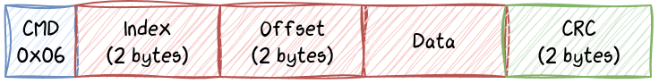
Read command
The Read command (0x05), visible in our earlier I2C capture, is a good example to illustrate the general command/response structure.
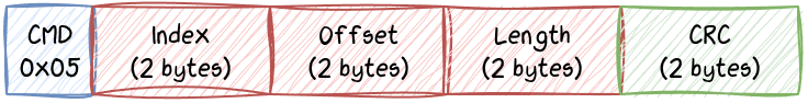
It reads data from a selected zone, with a given offset and length, and requires a CRC16 for validation. The command parameters are:
- Index → selects the data zone:
- 0: Device certificate
- 1: Manufacturer certificate
- 2: Root certificate
- 3: Product data
- 4: User data
- Offset → starting position within the selected zone;
- Length → number of bytes to read (capped because the response cannot exceed 512 bytes).
Note that all three certificates available here are public certificates, the corresponding private keys are never exposed over I2C. The host can read the chip's identity and verify its certificate chain, but the private key material stays inside the chip and is only used internally by the cryptographic commands (Generate signature, Establish key). This is exactly the trust boundary a secure element is meant to enforce.
We tried to read outside of these defined zones, but the chip consistently returned an error in those cases.
Command response
All commands return a response with the following structure:
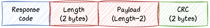
The response status can take several values, including:
0x00→ OK0x01→ Invalid CRC0x02→ Invalid arguments0x04→ Unsupported command0x06→ Length too large- ...
To make this concrete, here is an actual exchange we observed for a Read command:
Request: READ (Index=3, Offset=2, Length=8, CRC=0x58EF)
Raw response: [ 00 | 000A | 00 00 00 00 41 FF E5 6F | 71C8 ]
Decoded response:
- Status: OK (
0x00); - Length:
0x000A; - Product ID:
0x41FFE56F; - CRC:
0x71C8.
This command reads the product ID of the device.
Testing
Until now we had only passively sniffed the communication with the secure chip. To go further, we needed to actively send our own commands.
Testing setup
For this, we used a third device that also embeds the MJA1 chip: the Xiaomi Camera C301, on which we had root access (see acknowledgments).
We developed a small C program that interacts directly through Linux's I2C userspace interface. It opens /dev/i2c-0, sets the slave address with an ioctl(fd, I2C_SLAVE, 0x2A), then issues plain write() and read() syscalls to exchange frames.
int fd = open("/dev/i2c-0", O_RDWR);
ioctl(fd, I2C_SLAVE, 0x2A);
write(fd, cmd, cmd_len);
read(fd, resp, resp_len);
Around this I/O core, we built a small dispatch table mapping each command name to a dedicated builder function (cmd_build_read, cmd_build_update, cmd_build_generate_signature, and so on). Each builder takes the high-level arguments, packs them into the format we had reverse engineered, and appends the CRC. This gave us a clean CLI for interactive testing:
$ ./mjac_send read 3 2 8        # READ zone=3, offset=2, length=8
$ ./mjac_send query             # query chip info
$ ./mjac_send custom 130000...  # send arbitrary frame for fuzzing
The program was cross-compiled using a Buildroot toolchain to match the camera's architecture and copied to the device over SSH.
One important limitation we ran into: after each command we sent, the chip became unresponsive and required a full device reboot to talk again. This did not happen during passive sniffing, suggesting that the issue is specific to active interaction.
We spent a fair amount of time trying to track it down. We tweaked our sending code in several ways: changing how the I2C transactions were issued through the kernel interface, splitting or combining read/write phases, adjusting delays between them, and captured each variant with the logic analyzer to compare it against captures of legitimate miio_client exchanges. Even with the same pattern, the chip still refused to talk after one successful transaction.
We never figured out the root cause. Despite this limitation, we could still send commands one at a time and observe the responses.
Brute-forcing command IDs
With an active testing setup in place, the next natural step was to look for undocumented or hidden commands that miio_client never references.
We iterated over all possible command IDs (0x00 to 0xFF), sent each one to the chip with a valid CRC, and observed the response code. Commands returning "Unsupported command" (0x04) were considered absent, while any other response was worth investigating.
To overcome the unresponsive chip limitation, we wrote a small Python controller running on our laptop that automates the full cycle for each command ID:
- Connect to the camera over SSH;
- Run our C testing program with the candidate command ID;
- Capture the response and log it;
- If the response indicates the chip is in its unresponsive state, issue a
rebootover SSH; - Wait for the device to come back online (by repeatedly trying to open an SSH connection);
- Move on to the next command ID.
This revealed two additional commands that were not in the list extracted from miio_client:
- 0x06 → Update: writes data to a zone (see below);
- 0x13 → Unknown: always returns an undocumented error code
0x0F.
Command 0x13 is the more intriguing of the two. It does not return "Unsupported command", but rather a custom error code, which suggests that the command exists and is partially handled, but that something prevents it from executing normally. It probably requires specific preconditions or arguments that we have not yet identified. Targeted argument fuzzing on this single command could be interesting for future work.
Update command (0x06)
The name of this command might suggest something related to firmware update, but in reality, it is not related at all. The Update command has the same structure as the Read command previously seen:
It writes data to a selected zone at a chosen offset, with CRC16 validation. However, after extensive testing we found that:
- Only the user data zone (Index=4) can actually be modified. All other zones (certificates and product data) are read-only;
- The data length is limited by the I2C buffer size;
- The offset is also bounded by the size of the user data zone.
In other words, the chip enforces strong write protection on the zones that matter most: the device, manufacturer, and root certificates as well as product data are all immutable from the host side.
Conclusion & next steps
Starting from a chip with zero public documentation, we identified its communication interface, dumped and reverse engineered the host-side firmware that talks to it, recovered the full format including its CRC variant, and brute-forced the command ID space to find two undocumented commands.
From the host side, the chip behaves correctly: certificates and product data are read-only, private keys never cross the I2C bus, writes are restricted to a user data zone, and malformed arguments are properly rejected. No obvious flaw at the protocol level — but the protocol is only the front door.
Several directions are now open for further research:
- Desoldering the chip to test it in isolation on a custom board powered by a microcontroller. This would remove the reboot-after-each-command limitation that hampered our active testing and enable proper fuzzing of all commands and arguments, including a deeper look at the mysterious
0x13command. - Fault injection (voltage glitching, EM pulse, clock glitching). The chip enforces strict access control on which zones can be read or written. What happens if a glitch is injected precisely when the chip is checking the zone index in a
Readcommand? Could the check be bypassed to read outside of the defined zones? For example, reaching the chip's internal memory, private keys, or firmware? - Side-channel analysis (power, EM). The chip performs ECC operations as part of
Generate key,Establish key, andGenerate signature. These are classic targets for power and electromagnetic side-channel attacks aiming to recover private key material.
The protocol-level analysis presented here is, in many ways, the easy part. The more interesting work begins once the chip can be physically isolated and analyzed through its analog side channels.
We hope this post serves as a useful starting point for anyone interested in extending this work into practical side-channel analysis.
Acknowledgments
Many thanks to Alexandre Chazal for sharing root access on the Xiaomi Camera C301, which made the active testing phase possible. Thanks also to my colleagues for reviewing this blog post, providing valuable feedback, and sharing insightful tips during the research phase.
If you would like to learn more about our security audits and explore how we can help you, get in touch with us!
如有侵权请联系:admin#unsafe.sh